[ Instrument R & D of Instrument Network ] In order to explore the nano world more intuitively, a large number of researchers are committed to developing micro-nano detection technology with high time-space resolution. A few days ago, the National Key Laboratory of Mesoscopic Physics, Peking University School of Physics, and the Optoelectronics Frontier Science Center Gong Qihuang's team of academicians successfully developed a femtosecond-nano-ultra-spatial-temporal resolution optical experimental system with the support of national major scientific research equipment development projects. The experimental system can achieve ultra-high temporal resolution of several femtoseconds and ultra-high spatial resolution of four nanometers at the same time, and it has become a powerful experimental measurement method for meteorology and micro-nano photonics research.
Recently, the research team used ultra-high time-space-resolved light emission electron microscopy (PEEM) to reveal for the first time the internal correlation between local field plasmon near-field enhancement and decoherence time from the near-field microscopic perspective. The two dimensions of population evolution fully reveal the single layer WS2 ultrafast electron cooling and relaxation dynamics.
In the surface plasmon photonics experiment, the advantage of the high spatial resolution of PEEM was used to directly observe the near-field distribution of the local surface plasmon mode in the gold nanostructure dimer array system. Light emission intensity measurement and ultrashort pulse-based light emission autocorrelation measurement, respectively, obtained the near-field enhancement and decoherence time of the surface plasmon of the same structure, and found that the correlation between the two depends on the gold nanostructure dimer The gap and the polarization direction of the excitation light reveal for the first time that this correlation is determined by the near-field and far-field coupling and the local effect of the nanostructure.
The research results are of great significance for understanding the basic physical problems in surface plasmon photonics and expanding the application research of surface plasmons in high-sensitivity detection and sensing, solar cells and other micro-nano photonic devices.
In the study of the ultrafast electron cooling and relaxation dynamics of single-layer WS2, the team found that two time-scale ultrafast dynamic processes that exist on the substrate and the suspended single-layer WS2 are attributed to the electron cooling of the conduction band, respectively And the defect capture process, two time-scale processes can be observed from the attenuation curve, which are about 0.3 ps and 3 ps, respectively. Through energy-resolved PEEM measurement, it was found that the first process corresponds to the cooling of electrons in the conduction band, and the second process reflects the relaxation of electrons at the bottom of the conduction band.
In addition, by comparing the PEEM measurement of the suspended single-layer WS2 sample, combined with the fluorescence and Raman spectroscopy characterization, it is found that the relaxation process is mainly related to the defect state. This study uses PEEM's resolution capabilities in space, time, and energy to reveal the dynamic process of ultra-fast electron cooling and defect trapping of typical single layer WS2 of TMDs. The study also found that the generation of defect states is related to the illumination under vacuum. The generation method of this defect and its significant impact on the dynamic process are notable in general light emission experiments and spectral measurements.
The related research work was completed by the team of Peking University, Professor Hiroaki Misawa, Institute of Electronic Science, Hokkaido University, Japan, and Researcher Tan Pingheng, the Institute of Semiconductor Research, Chinese Academy of Sciences. Peking University doctoral student Li Yaolong is the first author of two articles. The research work has obtained the key research and development plan of the Ministry of Science and Technology, the National Natural Science Foundation of China, the State Key Laboratory of Artificial Microstructures and Mesoscopic Physics, the Collaborative Innovation Center for Quantum Matter Science, the Collaborative Innovation Center for Extreme Optics and the Frontier Science Center of Nanoelectronics, and the Ministry of Science and Technology Support from the Provincial and Japan Academic Promotion Association.
After more than 50 years of development, the electron microscope has become an indispensable and important tool in modern science and technology. The electron microscope is composed of three parts: lens barrel, vacuum device and power cabinet. Its technical application is based on the optical microscope, the resolution of the optical microscope is 0.2μm, and the resolution of the transmission electron microscope is 0.2nm, which means that the transmission electron microscope is magnified 1000 times on the basis of the optical microscope .
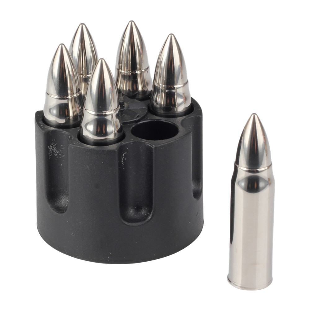
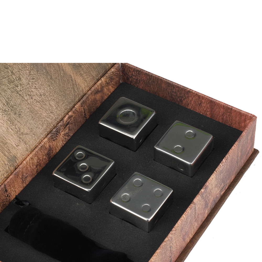
Stainless Steel Whiskey Stone
Whiskey Stone
High
quality whiskey stone ,help you enjoy the cold wine. Please out it in the ice
box for some time first before use it. Different shape for you to choose, ice
cube, diamonds ball , bullet shape and so on. Some items with the ice tong,
bundle pocket, Really suitable for take out for use. The material of the whiskey
stone is SS304, which is food grade with excellent quality.
So many
items for you to choose,2pcs/ 4pcs/ 6pcs/ 8pcs items.
Welcome
to choose the suitable one and contact us for the quotation, will be glad to
hear from you.
Material:SS304
Finishing:
Satin polishing ,Mirror Polishing ,Color painting
Logo:
Laser logo, Etching logo, Silk printing logo, Embossed logo, Decal logo
MOQ :
2000 PCS
Packaging
: White box, Mail box or Customized package
Sample
Time : 7~10 days
Lead Time
:60 days after have the deposit
Payment:
T/T ,L/C or others
Payment
term: 30% deposit before production and 70 % balance against the copy B/L


FAQ:
1:How can I get the sample?
We can provide the sample for
customers to check the quality.
Please kindly provide the delivery
info for calculate the sample cost. If you have DHL /TNT/UPS/FEDEX account,
please also kindly provide it to us.
You can do the payment of sample
via T/T and PayPal.
2:How about the sample time?
Usually the sample time is 7~10
days after have the sample cost.
3:How long will it take for mass
production?
Usually 45~60 days after have the
deposit.
4:Can we have our logo or company
name to be printed on your products or the package?
Welcome OEM.
5:what certificate can you provide?
CE,CB,GS,FDA,LFGB,ROHS are
available here.
6:How can we get your monthly new
products announcement?
Please join our mailing lists.
Our Service
Excellent quality
OEM packaging and product
Good service
Rich experience save your time and money


